Research Program
Spin and angle resolved photoemission of low dimensional materials
[대표 논문] “Surface Mott insulator on top of a trivial quasi two dimensional bulk insulator 1T-TaS2” submitted
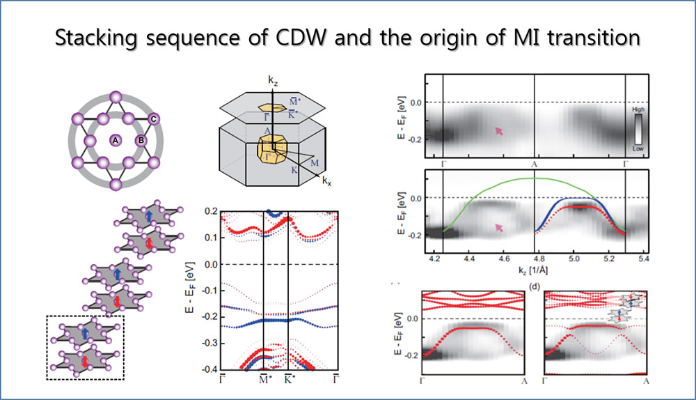
The quasi two dimensional charge density wave system of 1T-TaS2 has been known as a Mott insulator with a possibility of quantum spin liquid, recent band structure calculations and spectroscopic works in parallel suggested a metallic system or a spin-singlet insulator due to the interlayer coupling. We investigated the out-of-plane electron dispersion with angle-resolved photoelectron spectroscopy and identified two distinct branches for the topmost valence band, which can be unambiguously related to the surface and the bulk layers with different band gaps. We clearly revealed that the bulk is a trivial band insulator by interlayer coupling between the superlattices of CDW and the surface is a Mott insulator by the electron correlation.
[대표 논문]"Elctrical Tuning of excitonic Iisulator ground state of Ta2NiSe5", Phys. Rev. Lett. 123, 206401 (2019)
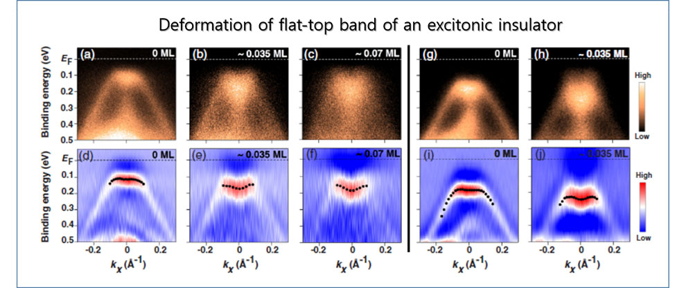
An electrical control of the excitonic insulator ground state of Ta2NiSe5 was demonstrated with the deposition of electropositive surface adsorbates. An intriguing wave-vector-dependent deformations of the characteristic flattop valence band of Ta2NiSe5 upon Potassium adsorption was observed with angle resolved photoemission. The band deformation indicates a reduction of the single-particle band gap due to the Stark effect near the surface. This study provides the foundation for the electrical tuning of the many-body quantum states in excitonic insulators.
 Center for Artificial Low
Dimensional Electronic Systems
IBS POSTECH Campus 79, Jigok-ro 127beon-gil, Namgu, Pohang, Korea, (37673)
Tel+ 82-54-260-9022
Copyright(c) Center for Artificial Low Dimensional Electronic Systems at IBS.All Rights Reserved.