About CALDES
Center Research Facilities and Equipment
-
ARPES can directly probe energy and momentum resolved electronic structures and our effort to construct a state-of-the-art ARPES station has been pursued largely in two directions: accessing all degrees of freedom of electrons and in-situ control of materials electronic phases. The construction of CALDES ARPES endstation at the nearby synchrotron radiation source (PLS-II) was started in 2014 by installing a brilliant elliptically polarized undulator (EPU) at existing beamline 4A. The modification of the beamline optical system was followed to make optimal use of the new undulator and the endstation was built in 2015-2016. Since then, the endstation has been open for outside users. Not only the band mapping in 3D crystal momentum space, but also the symmetry characterization of a specific band became available using variously-polarized photons from the EPU in a wide photon energy range [Nature Phys. 2017]. After the successful operation of the ARPES system, we moved to the challenge of measuring the 3D spin-orientation of photoelectrons efficiently through developing our own VLEED spin detector. This detector utilizes strong exchange scattering of electron spins at low energies with a ferromagnetic target and is known to be far more efficient than the conventional Mott spin detector. The first spin-polarized spectrum with the VLEED detector was obtained in 2019, and it took a few more years of effort to optimize and stabilize the performance due mainly to the very high sensitivity of low-energy electrons and the target surface. The performance of the spin detector, which is ready for practical measurements in 2023, was demonstrated by the angle-resolved spin texture measurement of a well known surface state of a topological insulator Bi2Se3 (see figure below) The angular scan was performed by the DA mode of the electron analyzer without any actual rotation of the sample and the spin asymmetry is set to be 0.3 to obtain all the spectra in a few hours.
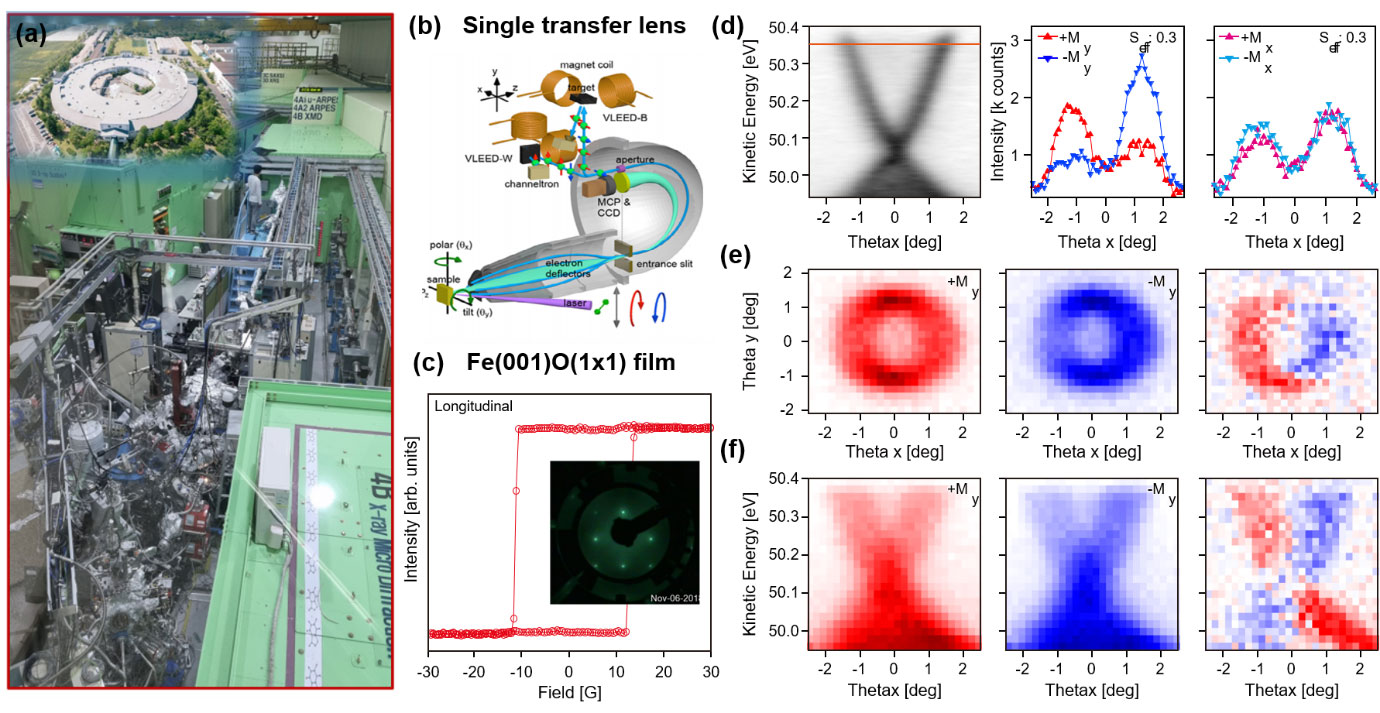
Figure J1. (a) The 4A undulator beamline of PLS. We have upgraded it by installing a new undulator for our spin-ARPES system. (b) Configuration of the transfer lens system and VLEED detectors for spin. (c) The characterization of a ferromagnetic scattering target of the detector. (d)(e)(f) Spin-resoved ARPES spectra obtained for the surface state of a topological insulator Bi2Se3.
Along with the spin detection, we developed various in-situ growth and treatment schemes for ARPES. In particular, to access phase transitions in a more systematic way, we have developed real-time evaporators and a laser-heating system. We have two evaporators aiming at the photon beam position on the sample and the ARPES data can be obtained while the dosing continues, whose replacement and degassing can be done without breaking the UHV condition of the main chamber. The laser-heating system allows us to raise the sample temperature up to 1200 K without any noticeable degassing. The heating can also be done at the photon beam position while the ARPES data are taken.
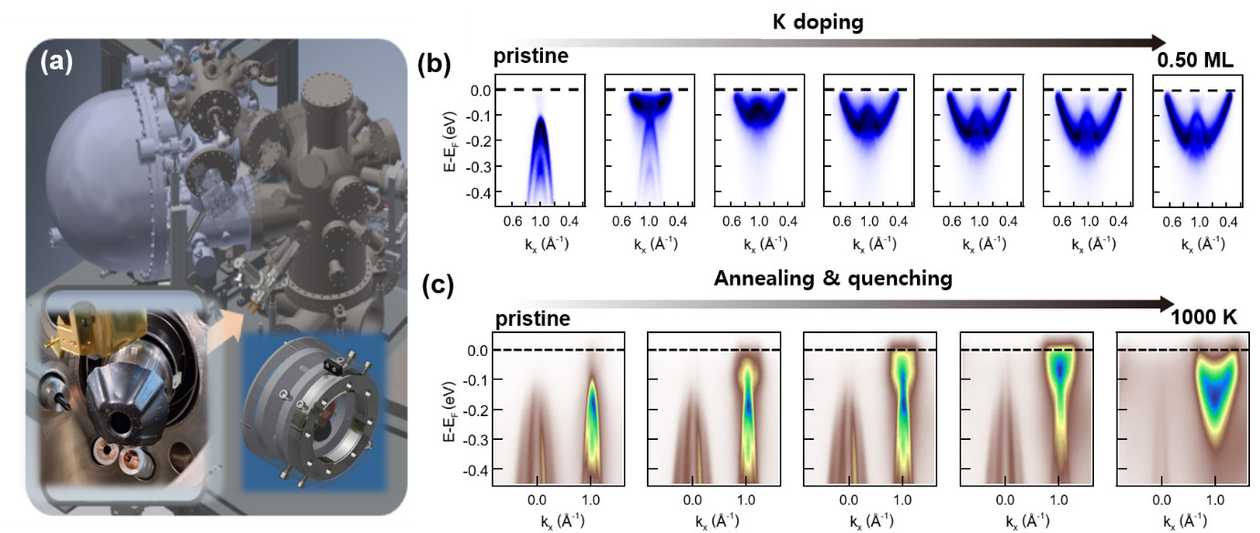
Figure J2. ARPES to capture artificially-controlled phases using (b) real-time doping and and (c) laser heating.
The ARPES data were obtained for the CDW transition of 1T-TiSe2.The CALDEs ARPES endstation has been very actively used by outside users through the user program of PLS. By the contract with PLS, we have 94 days of beamtime in a year and half of them are allocated to external user proposals. We are in charge of external user support too. After the official opening in late 2016, the number of users has grown steadily. In total, we supported 89 external user runs including 6 user groups from overseas. While the increase of overseas users has been heavily limited by COVID19 situation, we expect that the completion of the spin detector will trigger a huge inflow of overseas users.
Year, 2016, 2017, 2018, 2019, 2020, 2021, 2022, 2023 Year 2016 2017 2018 2019 2020 2021 2022 2023 proposals 5 10 14 13 20 22 20 21 allocated 4 10 10 9 13 15 14 14 oversea 0 0 1 1 2 1 0 1 Competition 1.25 1.00 1.40 1.44 1.54 1.47 1.43 1.50 Table J1. External users of the spin-ARPES system through the Pohang Accelerator Laboratory User program (2016-2023).
-
Since the physical properties of 1D/2D emerging phases depend crucially on various low-energy excitations, the ARPES measurements of the electronic structure around Fermi level are essential. Synchrotron-radiation ARPES is powerful in terms of controllable photon energy and polarization, but its practical energy resolution is limited to a few meV, not sufficient to resolve low-energy quasi-particles and resonance features. To go beyond this limit and also to alleviate the heavy beamtime request in the synchrotron, we have developed an extra ARPES setup adopting an 11-eV laser. This source offers a high photon flux within a narrow bandwidth of 0.1 meV. The laser is combined with a-state-of-art electron analyzer, which has a wider acceptance angle to cover a full Brillouin zone of most transition metal dichalcogenide materials with sufficient momentum resolution. The system was assembled in 2021 and the first ARPES data was taken in the middle of 2023 after two years of commissioning and the move to the new building.
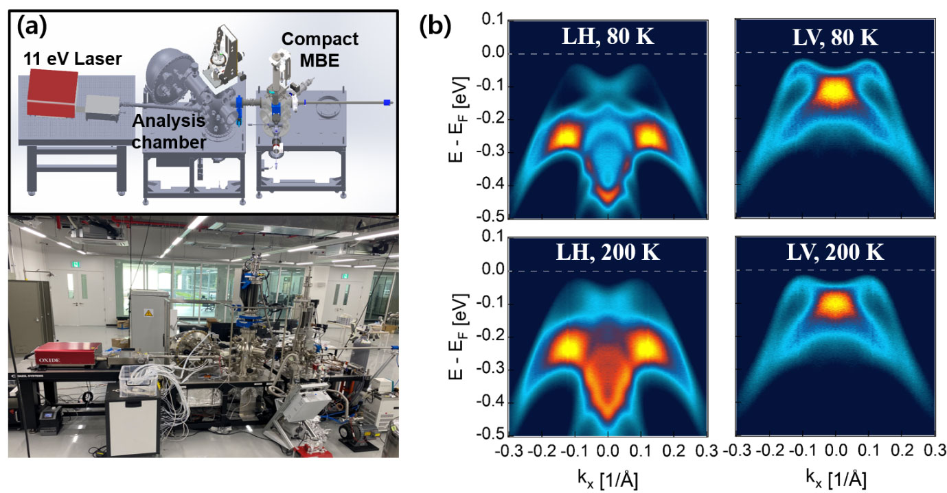
Figure J3. (a) 11-eV laser ARPES setup, which is combined with a compact MBE to access in-situ grown materials, too.
(b) ARPES data of an excitonic insulator candidate Ta2Pd3Te5 taken with extreme resolution and varied polarization/temperature. -
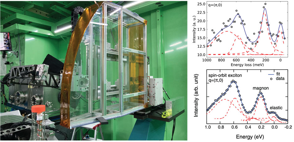
Figure J4. RIXS spectrometer and test spectrum compared to data taken at APS.
Resonant inelastic x-ray scattering (RIXS) has recently emerged as a powerful tool to probe energy- and momentum-resolved dynamics of elementary excitations. RIXS is particularly well suited for studying spin and orbital dynamics of correlated magnetic materials. Our center constructed the first RIXS spectrometer in Korea at the 1C beamline of Pohang Light Source. RIXS spectrometer consists of an analyzer crystal and a strip detector mounted on a 1-m radius Rowland’s circle geometry and is equipped with a 4-circle diffractometer and a 4-K cryostat. Its performance was verified by measuring the spin-wave excitation of Sr2IrO4 (see figure below) to feature an energy resolution of 40 meV. Currently, the limiting factor of the energy resolution appears to be the beam footprint size on the sample position. Our RIXS spectrometer was made open to general users from 2022.
-
Since 2014, we have developed an STM, which can study electronic states at centi-K (below 0.1 K in electron temperature) and high magnetic field (up to ~10 Tesla). The development included the construction of a dedicated building, a vibration isolation facility with 40 tons of passive damping block, and the connection to a He liquefier of Pohang Light Source during 2014-2017. The STM construction was started with a UHV dilution refrigerator from 2018 but was finished only in 2023 due partly to a long delay in the delivery/repair of the refrigerator during the COVID-19 period. At present, the world-record-level electron temperature of 7.3 cK was achieved, which is at the same level as the recently-built dilution-refrigerator-STMs in MPI Stuttgart (Kern group), NIST (Stroscio group), and RIKEN (Hanaguri group). From 2024 March, the STM is planned to be used for three flagship experiments utilizing its unprecedented temperature and energy resolution. The experiments include (i) the spectroscopic study of gapless quantum spin liquids in a van der Waals system, (ii) the spatial investigation of pair density waves in 2D van der Waals superconductors, and (iii) the STM manipulation of non-Abelian anions in the fraction quantum Hall states of bilayer graphene. The last experiment was proposed by the Center for van der Waals Quantum Solids and will be the first inter-center collaboration project within the IBS Institute for Condensed Matter Science.
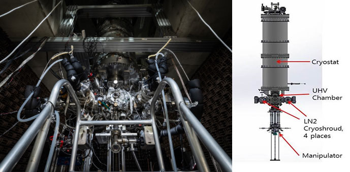
Figure J5. Bottom view of the centi-Kelvin high magnetic field STM (left) and its schematics (right).
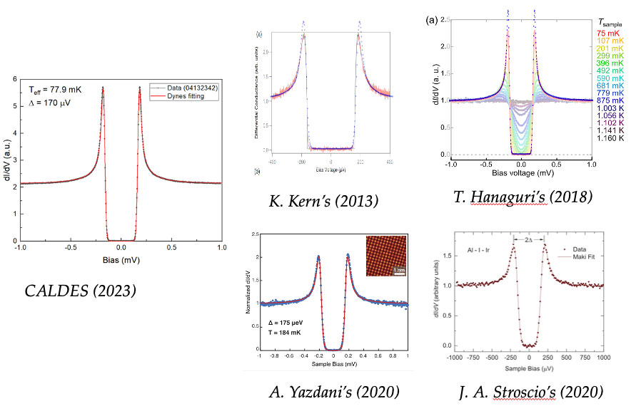
Figure J6. Comparison of scanning tunneling spectroscopy spectra for the superconducting gap of Al for major ultra-low-temperature STMs in Germany, Japan, and USA. Our data (Left, fitted to have an effective electron temperature of 77 mK) was overlaid onto the data of Kern and Hagaguri groups’ (Top right, the data in blue dots are our data).
-
We have constructed a low-temperature high-field scanning probe microscope, which can operate as both an atomic force microscope (AFM) and a scanning tunneling microscope (STM) under extreme conditions (2 K, 12 T). This system's mission is to extend the magnetic field range of our conventional STM from 3 to 12 T and to make possible the atomic-resolution probe microscopy (AFM) on non-metallic samples (using the quartz tuning fork tips). The system is also equipped with in-situ surface treatment techniques, such as low-temperature cleaving and thermal deposition at variable temperatures, to investigate various artificial low-dimensional electronic systems fabricated in different ways. After confirmation of ultra-low temperature and high magnetic field operation of atomic resolution AFM and STM, the system was moved to our new building and is under experiments.

Figure J7. (a) ULT-HF-SPM (inset) a quartz tuning fork with a W tip. (b, c) atomic resolution AFM images of (b) Si(111) and (c) Pb(111). (d) Superconducting gap of Pb in tunneling spectroscopy.
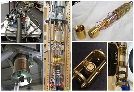
Figure J8. (left) high-magnetic-field/dilution-refrigerator and the measurements systems (middle) the dilution-refrigerator part
(right) Sample probes with electrical filters and two-axis and one-axis rotators.Operation and upgrade of high field magnet/dilution refrigerator system:
The high field magnet/ dilution refrigerator system, installed in 2015 in IBS-CALDES, offers extreme conditions of high magnetic field of B = 20 T, the largest magnetic field in Korea, and low temperature down to T = 10 mK simultaneously. This unique condition of high B/T ratio can be combined with diamond anvil cell for high pressure up to P = 40 GPa, with a two-axis rotator probe for controlling the applied magnetic field to any desirable directions, and with electrical filtering for low-noise precision measurements. These unique facilities for multiple extreme conditions have been used to investigate various physical properties, including magnetic quantum oscillations, nonreciprocal electrical transport, thermoelectric/thermal transport, specific heat, and torque magnetometry, on various low-dimensional quantum materials such as topological semimetals, frustrated magnets, and unconventional superconductors. A few representative achievements are detection of spin-splitting Landau levels of nodal-line fermions [Nat. Commu. 2022], discovery of colossal angular magnetoresistance [Nature 2021], pressure-induced metal-insulator transition [Nat. Commun. under review]. Currently, this facility is actively used by the researchers in CALDES as well as external users from other IBS centers and several groups in other universities (POSTECH, Seoul Nat. Univ. Ewha Womans Univ., Kyungpook Nat. Univ., DGIST, Pusan Nat. Univ. etc.) and companies (Kiswire Advanced Technology, etc.) in Korea. -
The vector-magnet/Raman spectroscopy system, installed in 2021 in CALDES, has been actively employed for investigation of phononic, magnonic and electronic excitations of low-dimensional quantum materials. Equipped with 9-2-2T vector magnet, this system allows for precise application of magnetic field in any desirable direction, and home-built Raman spectrometer enables high resolution of 0.1 meV, an excellent signal-to-noise ratio, and access to low energy transfer down to 1 meV, along with various wavelength and linear/circular polarizations. Various quantum materials, including van der Waals magnets, excitonic insulators [Nature Commun. 2021], topological semimetals, and strong spin-orbit-coupled magnets [Nature 2024], have been investigated to identify their phonon, exciton, magnon excitations. This facility has been internally used by researchers in CALDES and POSTECH, but is poised to open to external users from other IBS centers and other universities in Korea. Additionally, recent completion of magneto-optical Kerr microscopy and magnetic circular dichroism microscopy setups further enhances the facility’s capability, with plans for operation in 2024.

Figure J9. High-field cryogenic Raman spectrometer.
-
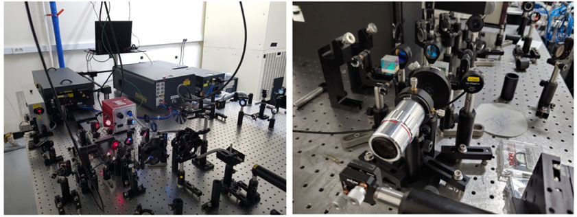
Figure J10. Femtosecond laser system for time-resolved spectroscopies and second harmonic generation.
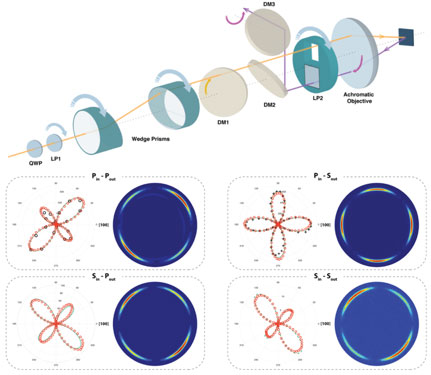
Figure J11. Schematic of our second harmonic generation setup and reference data taken on GaAs.
Ultrafast time-resolved optical spectroscopy allows investigation of transient non-equilibrium states of matter and we have outsourced this field of research to the time-resolved spectroscopy group in Seoul National University. After the joining of a new PI, J. H. Kim from the department of materials science POSTECH with the expertise in this field, we started to construct a setup consisting of the femto-second laser system and optical parametric amplifiers capable of generating pulses as narrow as 40 fs and a wide range of wavelengths from ultraviolet ~330 nm to far-infrared ~ 20,000 nm. In addition, we have constructed non-linear optics setups for the symmetry analysis of materials. The setup detects high harmonic generation from the specimen, which has high sensitivity to changes in anisotropy and symmetry of a crystal. Our setup is a modification of the scheme invented by Hsieh group (Caltech), which allows probing small bulk single crystals at the μm length scale, sensitivity to the entire nonlinear optical susceptibility tensor in oblique light incidence reflection geometry.
-
Following the completion of the new IBS center building in 2023, we proceeded with the establishment of clean-room facilities (CLASS 100) dedicated to device fabrication. These facilities house state-of-the-art equipments, including an electron-ion dual-beam lithography machine, a wet station for chemical treatments, and a glove box equipped with transfer stages for the exfoliation and stacking of various two-dimensional materials. One of the main equipments is the electron-ion dual-beam lithography machine for high-resolution electron beam lithography capability, which enables the stable fabrication of intricate patterns with resolutions down to the 100 nm range as shown below. Furthermore, focused-ion milling (FIB) and deposition (GIS) techniques employing a stabilized focused ion beam have been instrumental in etching various single crystals and fabricating electrode patterns. Presently, etching and fabrication processes of diverse single crystals such as PdCrO2, SrAs3, YMn6Sn6, and Sr2IrO4 have been carried out, which enables precise shaping of single crystals to desired orientations and thicknesses, and subsequently depositing electrodes with low contact resistance at room temperature. We have also developed a novel technique utilizing FIB to etch specific portions of single crystals to desired orientations, subsequently placing resulting microcrystals onto substrates for further etching and electrode deposition. Currently, a team of 30 researchers from both internal and external research groups utilize these cutting-edge tools, primarily focusing on fabricating devices using low-dimensional materials.
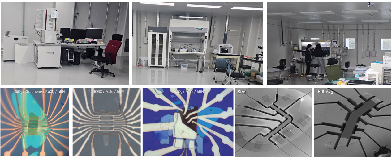
Figure J12. Upper panel, Pictures for clean room facilities in a new IBS center building. Lower panel Optical images for low-D material-based electronic devices and SEM images for FIB-etched single crystals with patterned electrodes.
 Center for Artificial Low