About CALDES
Mission
As one of research centers of the Institute of Basic Science, the Center of Artificial Low Dimensional Electronic Systems will conduct world-class research based on our previous experience of atomic scale control in low-dimensional materials as well as characterization techniques, which were accumulated through Center for Atomic Wires and Layers. We will provide creative idea to tune sophisticatedly properties of materials at the atomic scale, to create new types of low dimensional topological materials, and to investigate topological order microscopically. From these ideas, we will pioneer a new direction in the study of low-dimensional topological materials that still remains in the exploratory stage, and this fundamental and advanced research will make us to become the world leader in this field. As a result, through this creative and excellent research, we will train the world-leading researchers in the field of condensed matter physics, especially surface and nano physics. It is our goal to improve dramatically the level of human resources and research level of Korean condensed material physics. The specific research goals are following.
- 1Create atomically controlled artificial materials such as wires, layers, ultrathin films, heterointerfaces, and multilayers, which can host novel low dimensional electronic systems.
- 2Establish methods for the ultimate atomic scale measurement and control over these materials to manipulate their local and global electronic properties.
- 3Discover new types of quantum matter originating from exotic symmetries, topology, and interactions of low dimensional electrons and challenge the grand problems of the quantum phase fluctuations, competitions, and transitions of low dimensional electrons.
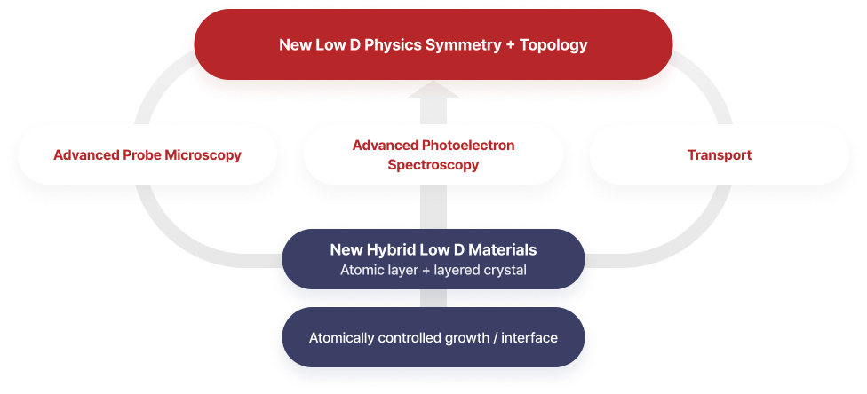
In achieving the above goals, we propose an innovative approach through the combination of atomically controlled in-and ex-situ growth of new materials with the advanced spectroscopic and microscopic techniques such as spin-and-angle-resolved photoelectron spectroscopy and ultra-low-temperature-high-magnetic-field scanning tunneling microscopy.
Finally, we hope to secure a route to revolutionary electronic or spintronic devices based on new types of quantum properties of electrons in low dimension.
Basically, we suggested that various new low dimensional topological materials can be found and fabricated and this direction has been proved to be extremely successful during last five years. Together with existing topological materials, there is huge room for discoveries when we investigate their edge electronic channels, especially with atom resolution probes. We can further create various different types of heterointerfaces between topological materials and materials with distinct symmetries and interactions. The research on these heterointerfaces of atomic layer low dimensional materials are on its early stage and we have a great chance to become a leading group. In particular, while other major groups are still working basically on semiconductor heterostructures, we moved to more exotic heterointerfacial systems with strong spin, orbit, electron interactions for new physics. The idea of proximity coupling of different interactions at such heterointerfaces is pursued throughout this project.
Since most of the current research on topological materials focuses 3D bulk materials or semiconductor quantum well structures, the current project on 1D/2D topological systems in atomic scale materials is rather unique. Moreover, the idea of proximity coupling in atomically controlled heterointerfaces to find new physics beyond the current scope of topological materials is original. We aim to make this idea successful and establish strong world leadership in this new field.

 Center for Artificial Low