Research Program
Physics group
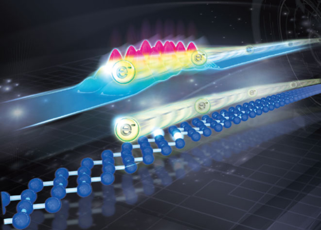
▲ Chiral soliton moving along an indium atomic wire (Science 2015 & Nature Physics 2017)
Director Han Woong Yeom’s group is mainly working with scanning tunneling microscopy/spectroscopy and angle-resolved photoelectron spectroscopy on surfaces and heterointerfaces of 1D and 2D materials systems. There are currently two major research programs.
▲ Chiral solitons in indium atomic chains and their chirality switching (Science 2015 & Nature Phys. 2017)
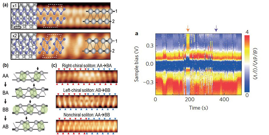
Our center has played a pioneering role in the atomic scale investigation of topological excitations in 1D and 2D materials. Our work in 2013 is the first direct microscopic observation of topological solitons and their electronic states in a 1D topological insulator, indium atomic chains on a silicon surface in its charge density wave state. In 2015, we clarified a novel Z4 topological nature of this system and the chiral nature of its solitons, writing a completely new chapter in the soliton physics. This work led us to find the chirality switching of the solitons, which represents the Z4 algebraic operation of solitons opening a possibility of using solitons for the robustly-protected multilevel information processing. Currently we are looking for a new class of solitons such as fractionally charged solitons (Z3 topology) and investigating the interactions between solitons, which would provide a wider and rich landscape in this research field.
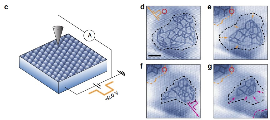
▲ Creating domain wall networks on a 2D material with strong electronic correlation, 1T-TaS2
(Nature Commun. 2016, 2017 & 2019).
On the other hand, from 2016, we successfully transferred the soliton research into 2D materials by creating and observing novel networks of topological excitations such as domain walls and their vortices in an unconventional 2D materials of 1T-TaS2. Solitonic domain walls in this system have a rich variety in their structures and electronic states, which are closely connected to unconventional electronic and magnetic properties of this system such as charge density wave, Mott insulating state, and spin frustraction. We believe that our original contribution to the investigation of domain wall networks of 2D systems with strong electronic correlation would reveal substantially new physics, which is also closely related to the outbreaking research field of twisted bilayer graphene.
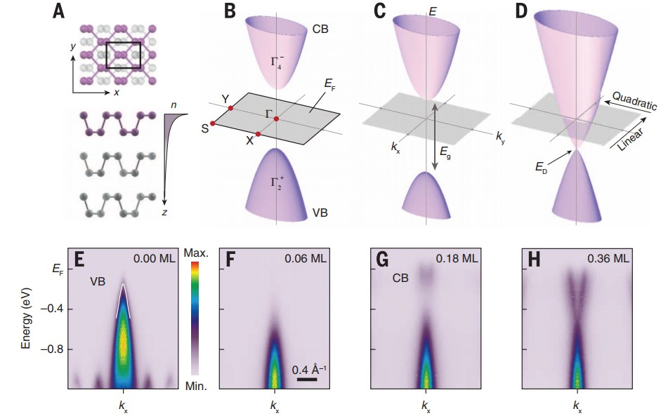
▲ Evolution of the band gap at the interface of a K/BP heterostructure (Science 2015)
One of our major proposals to possibly produce new quantum phases and functionalities is utilizing proximity interactions at interfaces of heterostructures of 1D/2D materials. In particular, we have focused on 2D materials with strong interactions such as electron correlation, electron-phonon interaction, or excitonic interactions. These strong interactions are to be enhanced and manipulated by proximity interactions at interfaces with other 2D materials and artificial structures. The materials picked up are 1T-TaS2 (and NbSe2) with strong electron correlation and electron-phonon interaction, IrTe2 with strong electron correlation and strong spin-orbit interactions, Ta2NiSe5 with strong excitonic interaction and electron-phonon interaction, and black phosphorous (BP) with topological degrees of freedom. We have tried to fabricate various atomic scale artificial structures and heterointerfaces on the surfaces of these materials. For example, superconducting Pb atomic layers and novel Pb clusters were grown on IrTe2 and Bi layers with strange topology was grown on BiSe2. The Pb clusters exhibit the formation of the rarely-observed relativistic molecular orbitals due to strong spin-orbit interaction, which we called as “artificial Dirac molecules.” We put atomic layers of akali metals on BP and Ta2NiSe5 to induce a unrealistically large Stark fields on their surface layers, which induce anisotropic Wyle semimetal in BP and tune the excitonic band gap in Ta2NiSe5. This research activity during last 5 years has been very successful and provided a strong proof of the concept and the methodology. We think that well designed heterointerfaces based on 2D materials with strong manybody interactions would provide a wide and wild possibility to find a plethora of novel quantum phenomena.
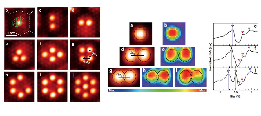
▲ Artificial Pb molecules with strong spin-orbit coupling as formed on the honeycomb charge order superlattice of IrTe2 (Nature Communications 2020).
For these research programs, we are operating six different STM machines currently with different operating temperatures, ranging from 0.9 K to 400 K) and different strength of magnetic fields (up to 12 Tesla), a home-lab ARPES system with a MBE set-up and a spin-resolved ARPES system connected to an ultrabright EPU in synchrotron-radiation source. At the same time, we are constructing a ultra low temperature STM system, which aims to reach 10 mK under a vector magnetic field of 2-2-9 Tesla.
- Dr. Jhinhwan Lee _ Cryogenic scanning probe microscopy and spectroscopy
- Low Temperature Scanning Tunneling Microscopy
- Spin and angle resolved photoemission of low dimensional materials
 Center for Artificial Low
Dimensional Electronic Systems
IBS POSTECH Campus 79, Jigok-ro 127beon-gil, Namgu, Pohang, Korea, (37673)
Tel+ 82-54-260-9022
Copyright(c) Center for Artificial Low Dimensional Electronic Systems at IBS.All Rights Reserved.