Prof.Jonghwan Kim
Light-matter interaction in of vdW 2D heterostructures and their optoelectronic devices
1. Ultrafast laser spectroscopy of vdW 2D heterostructures
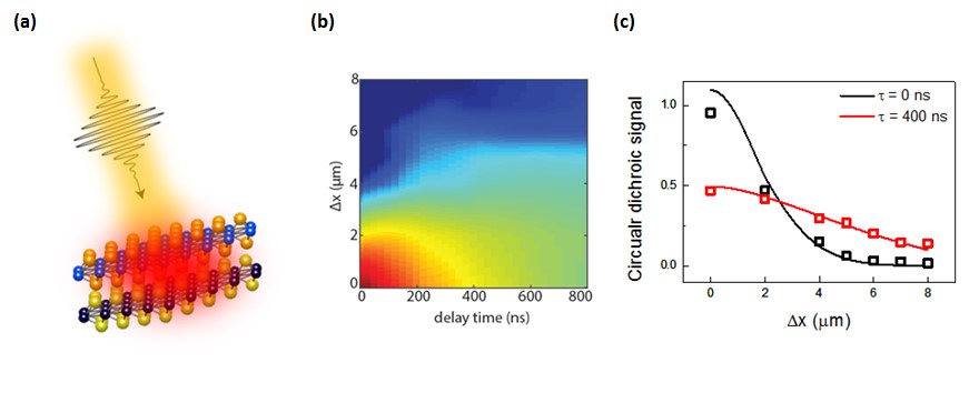
[대표 논문] Imaging of pure spin-valley diffusion current in WS2-WSe2 heterostructures, Science 360, 893-896 (2018).
Van der Waals heterostructures of atomically thin two-dimensional (2D) crystals are a new class of material in which novel quantum phenomena can emerge from layer–layer interactions. Electron–electron interactions between adjacent 2D layers can give rise to a variety of fascinating physical behaviours. The interlayer moiré potential between the graphene and hBN layers leads to mini-Dirac cones and the Hofstadter’s butterfly pattern in graphene/hBN heterostructures. Electronic couplings between MoS2 and MoS2 layers lead to a direct- to indirect-bandgap transition in bilayer MoS2 and Coulomb interactions between MoSe2 and WSe2 layers lead to interlayer exciton states in MoSe2/WSe2 heterostructures.
Here, we employ femtosecond laser spectroscopy to investigate novel electronic structure and phenomena in vdW heterostructures. For example, we used a heterostructure made out of adjacent layers of WSe2 and WS2 to create a spin-valley diffusion current without applying an external electric field. Instead, they used circularly polarized laser light to initiate the diffusion and a second laser pulse to image the propagation of the carriers. With long lifetimes and diffusion lengths, the method may be of practical use in future valleytronic devices.
2. Optoelectronic Devices of vdW 2D heterostructures
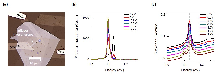
[대표 논문] Electrical control of anisotropic and tightly bound excitons in bilayer phosphorene, Phys. Rev. B 103, L041407 (2021).
2D vdW semiconductors have emerged as a unique platform for fascinating new optoelectronic applications. The strong light-matter interaction leads to the efficient light emission or absorption properties in the broad energy range from infrared to visible frequency depending on the size of the bandgap as shown for transition metal dichalcogenides and black phosphorus. Vertical integration with other 2D vdW materials further enables the injection or collection of charge carriers via atomically thin insulators of tunneling barriers and conductors, which provides highly efficient and tunable device architectures for light-emitting diodes, photovoltaics, photosensors and electro-optic modulators. Recent progress on the wafer-sized growth with high crystallinity suggests that these opportunities might be even available for scalable technological applications.
In our group, we demonstrate novel optoelectronic devices based on 2D vdW heterostructures. For example, we fabricate a field-effect transistor of bilayer phosphorene where light emission and absorption from strongly-bound and anisotropic excitons. Reflection contrast and photoluminescence spectroscopy shows the linear-dichroic optical spectra from anisotropic excitons and trions in the hBN-encapsulated bilayer phosphorene. The optical resonances from the exciton Rydberg series indicate that the neutral exciton binding energy is over 100 meV even with the dielectric screening from hBN. The electrostatic injection of free holes enables an additional optical resonance from a positive trion (charged exciton) ∼30 meV below the optical band gap of the charge-neutral system. Our work shows exciting possibilities for monolayer and few-layer phosphorene as a platform to explore many-body physics and photonics and optoelectronics based on strongly bound excitons with twofold anisotropy.

![]()
IBS POSTECH Campus 79, Jigok-ro 127beon-gil, Namgu, Pohang, Korea, 37673
Copyright(c) Center for Artificial Low Dimensional Electronic Systems at IBS.All Rights Reserved.